+86-574-87459965
+86-18858061329


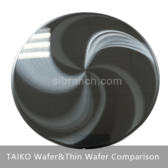
300mm TAIKO Wafer&Thin Wafer Comparison
TAIKO Wafer Grinding vs. Thin Wafer Processing: Key Advantages & Supporting Technologies
TAIKO Grinding Technology: A Breakthrough in Semiconductor Manufacturing
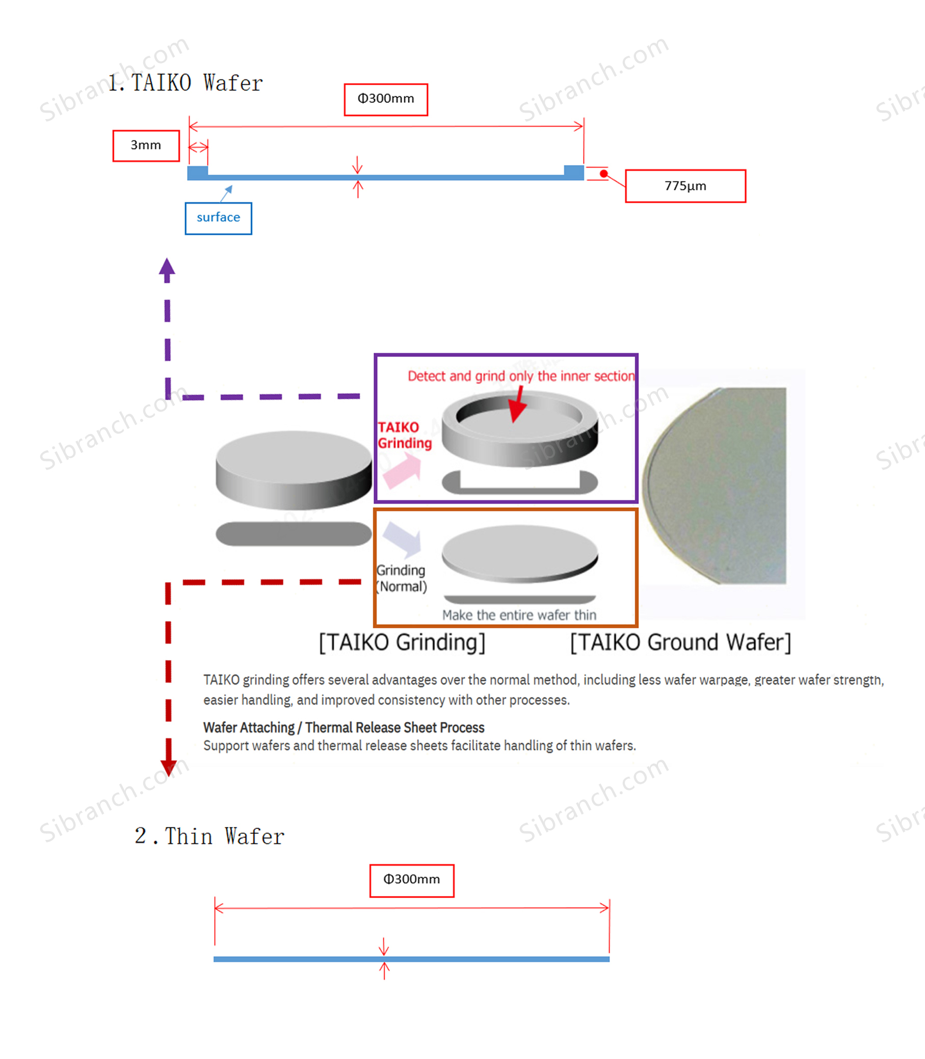
TAIKO grinding, an innovative wafer thinning process developed by DISCO Corporation, represents a significant advancement over conventional back-grinding methods. This technology thins the central area of the wafer while preserving a thick outer ring, offering substantial benefits for handling and processing thin wafers, particularly in advanced packaging and 3D integration applications.
Core Advantages of TAIKO Grinding Technology
1. Reduced Wafer Warpage
By maintaining a rigid outer ring, TAIKO grinding minimizes stress-induced warpage during and after thinning. This results in superior flatness, which is critical for photolithography, bonding, and other downstream processes, ultimately improving yield and device performance.
2. Enhanced Mechanical Strength
The thick periphery acts as a structural frame, significantly increasing the wafer's overall strength. This allows safer handling, transportation, and processing of ultra-thin wafers (down to <100µm) with drastically reduced risk of cracking or breakage.
3. Simplified Handling and Logistics
TAIKO-processed wafers can be handled using standard automated equipment designed for normal thickness wafers. This eliminates the need for expensive, specialized thin-wafer handling tools and simplifies integration into existing fabrication and packaging lines.
4. Improved Process Integration and Consistency
The standardized edge profile ensures better compatibility with wafer chucks, carriers, and process tools. This leads to more consistent results in subsequent steps such as deposition, etching, and cleaning, enhancing overall process stability.
Critical Supporting Technology: Temporary Bonding & Debonding
The Role of Carrier Wafers
For ultra-thin wafer processing (often below 50µm), temporary bonding to a rigid carrier (or support) wafer is essential. This technique provides mechanical support during backside grinding, handling, and backside processing, preventing damage to the fragile device layer.
Thermal Release Tape/Layer Process
A Thermal Release Sheet (or tape) is a key material in this temporary bonding process. It provides strong adhesion at room temperature for processing stability but loses its adhesive property upon heating to a specific temperature (typically 150-200°C), allowing clean, residue-free debonding of the thinned device wafer from the carrier.
Comparative Analysis & Integrated Process Flow
TAIKO vs. Conventional Thinning: Performance Comparison
Warpage Control: TAIKO (<50µm) vs. Conventional (150-300µm)
Minimum Achievable Thickness: TAIKO (enables <50µm) vs. Conventional (limit ~80-100µm)
Breakage Rate: TAIKO reduces breakage by over 60%
Equipment Compatibility: TAIKO wafers use standard tools vs. Conventional often requiring specialized thin-wafer tools
Integrated Manufacturing Solution
A complete thin-wafer solution often combines both technologies:
Temporary Bonding: The device wafer is bonded to a carrier wafer using a thermal release adhesive.
TAIKO Grinding: The stack is thinned using the TAIKO method, achieving target thickness with a supportive rim.
Backside Processing: Steps like metallization, via etching, or inspection are performed.
Debonding: The stack is heated to release the thin device wafer from the carrier.
Industry Applications & Future Trends
Key Application Areas
3D IC Packaging & Through-Silicon Vias (TSV): Enables reliable handling of ultra-thin wafers essential for vertical stacking.
CMOS Image Sensors (CIS) for Backside Illumination (BSI): Requires extreme thinning for optimal light sensitivity.
Power Devices: Thinner wafers reduce ON-resistance and improve thermal performance.
Flexible & Wearable Electronics: Provides robust, ultra-thin silicon substrates.
Technology Evolution
Material Development: Next-generation thermal release materials with lower activation temperatures for heat-sensitive devices.
Process Integration: Development of cluster tools combining bonding, grinding, and debonding for higher throughput.
Advanced Metrology: In-situ stress and thickness monitoring for real-time process control.
Sustainability: Focus on reusable carrier wafers and recyclable materials to reduce cost and waste.
TAIKO grinding technology, combined with temporary wafer bonding using thermal release materials, provides a robust solution for manufacturing and handling thin wafers. Key benefits include reduced wafer warpage, increased strength, easier handling, and better process integration. This combination is vital for advanced semiconductor applications like 3D packaging, image sensors, and power devices. As the industry continues to drive toward thinner, more compact, and higher-performance chips, TAIKO and supported thin-wafer processes will remain critical enabling technologies.


